LS700 (Atlanta)
Motherboard
 
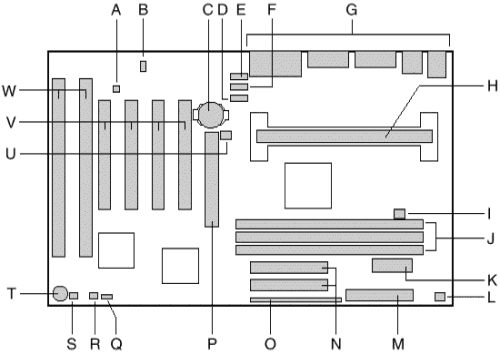
Motherboard Components
 |
| A |
Optional chassis security connector |
M |
Floppy drive connector |
| B |
Optional 'Wake on LAN' connector |
N |
IDE connectors |
| C |
Battery |
O |
Front panel connector |
| D |
Optional Line In connector |
P |
Accelerated Graphics Port (AGP) connector |
| E |
Optional CD-ROM audio connector |
Q |
Configuration jumper block |
| F |
Optional telephony connector |
R |
Optional SCSI hard disk LED connector |
| G |
Back-panel I/O connectors |
S |
'Wake on Ring' connector |
| H |
Slot 1 connector |
T |
Speaker |
| I |
Fan 3 header connector |
U |
Fan 2 connector |
| J |
DIMM sockets |
V |
PCI connectors |
| K |
Primary power connector |
W |
ISA connectors |
| L |
Fan 1 connector |
|
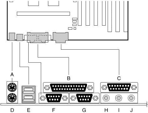
Back Panel I/O Connectors
 |
| A |
PS/2 connector (mouse or keyboard) |
F |
Serial port 1 connector |
| B |
Parallel port connector |
G |
Serial port 2 connector |
| C |
MIDI/game port connector |
H |
Audio line out jack |
| D |
PS/2 connector (mouse or keyboard) |
I |
Audio line in jack |
| E |
USB connectors |
J |
Audio mic in jack |
 
RAM Configuration
You can install from 8MB to 384MB of memory in the motherboard DIMM
sockets. There are three DIMM sockets arranged as banks 0, 1, and 2. The motherboard
supports the following memory features:
- 168-pin 3.3V DIMMs with gold plated contacts
- 66MHz unbuffered SDRAM
- Non-ECC (64-bit) or ECC (72-bit) memory
- 8MB, 16MB, 32MB, 64MB, and 128MB modules
When adding memory, follow these guidelines:
- You can install DIMMs of any size in any of the three banks.
- The BIOS detects the size and type of installed memory.
- For ECC operation, all installed memory must be ECC (72-bit) and you must
enable the ECC Configuration feature in the Setup program.
| SDRAM memory expansion for LS700 (Atlanta) Systems |
| 16MB 64-bit DIMM Module |
XB61385 |
| 32MB 64-bit DIMM Module |
XB61386 |
| 64MB 64-bit DIMM Module |
XB61387 |
| 128MB 64-bit DIMM Module |
XB61388 |
 
Disk Drives
| Hard Disk Drives |
| MB |
Make |
Model |
Type |
Part Number |
| 3.2GB |
Quantum |
ST3240A |
IDE |
SU61671 |
| 4.3GB |
Quantum |
ST4320A |
IDE |
SU62667 |
|
| Floppy Drive |
| MB |
Make |
Model |
Type |
Part Number |
| 2 MB |
Teac |
FD-235HG |
3.5" |
16259831 |
|
| CD-ROM |
| Speed |
Make |
Model |
Type |
Part Number |
| 24 |
Sony |
CDU621-10 |
IDE |
XB62488 |
 
Jumper Settings
Note that with this motherboard the setting of the processor clock speed
and clearing of passwords is carried out by software and not by hardware jumper settings,
via a Maintenance menu in Setup.
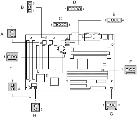
To enable this mode of Setup, a Configuration Jumper Block (J8B2) is set
as explained below. The diagram shows the location of the Configuration Jumper Block on
the motherboard. The jumper is set to normal mode at the factory.

The following table shows the jumper settings for the different Setup
modes. These modes configure Setup for normal operations, maintenance operations, or
recovering the BIOS.
| Function |
Jumper J8B2 |
Description |
| Normal |
1-2 |
BIOS uses current configuration and passwords for booting. |
| Configure |
2-3 |
After the POST runs, Setup starts and displays the Maintenance menu.
This menu displays options for setting the processor speed and clearing passwords. |
| Recovery |
None |
BIOS recovers data from a recovery diskette. |
 
Motherboard Connections

The connection details for these connectors are shown in the following
tables.
Chassis Security Connector (J2B1)
| Pin |
Signal Name |
| 2 |
Ground |
| 3 |
CHS_SEC |
Wake on LAN Connector (J1C1)
| Pin |
Signal Name |
| 1 |
+5 VSB |
| 2 |
Ground |
| 3 |
WOL |
ATAPI CD-ROM Audio Connector (J1F1)
| Pin |
Signal Name |
| 1 |
CD_IN-Left |
| 2 |
Ground |
| 3 |
Ground |
| 4 |
CD_IN-Right |
ATAPI-Style Telephony Connector (J2F1)
| Pin |
Signal Name |
| 1 |
Audio Out (monaural) |
| 2 |
Ground |
| 3 |
Ground |
| 4 |
Audio In (monaural) |
ATAPI-Style Line In Connector (J2F2)
| Pin |
Signal Name |
| 1 |
Left Line In |
| 2 |
Ground |
| 3 |
Ground |
| 4 |
Right Line In (monaural) |
Fan 3 Connector (J5L1) (Active Heatsink Fan)
| Pin |
Signal Name |
| 1 |
Ground |
| 2 |
+12V |
| 3 |
Ground |
Fan 1 Connector (J8M1)
| Pin |
Signal Name |
| 1 |
Ground |
| 2 |
FAN_CTRL (+12 V) |
| 3 |
FAN_SEN* |
* If the optional management extension hardware is not available, pin 3
is ground.
SCSI Hard Drive LED Input Connector (J8B1)
| Pin |
Signal Name |
| 1 |
DRV_ACT# |
| 2 |
No connect |
Wake on Ring Connector (J8A1)
| Pin |
Signal Name |
| 1 |
Ground |
| 2 |
RINGA |
Fan 2 Connector (J3F1)
| Pin |
Signal Name |
| 1 |
Ground |
| 2 |
FAN_CTRL (+12 V) |
| 3 |
FAN_SEN* |
* If the optional management extension hardware is not available, pin 3
is ground.
Audio Subsystem
The onboard audio subsystem is based on the Yamaha OPL family of
single-chip audio controllers (YM 715). The audio subsystem provides the digital
audio and analog mixing functions needed for recording and playing sound on personal
computers. The subsystem features:
- Line and microphone level inputs
- MIDI/Game port
- 3-D enhanced stereo
- Full digital control of all mixer and volume control functions
- Full duplex operation
- Sound Blaster Pro, Windows Sound System, Roland MPU-401, AdLib, and
Multimedia PC Level 2 (MPCII) compatibility
- Onboard Yamaha YM 704 wavetable synthesizer (optional)
- Wavetable upgrade connector
- CD-ROM audio connector
- Telephony connectors
Hardware Monitor Option
The hardware monitor option features the following:
- An integrated temperature sensor
- Fan speed sensors
- Power supply voltage monitor
- POST test result and error code storage
- Support for Intel LANDesk� Client Manager
- Connector for external chassis security feature
These features are implemented by an integrated hardware monitor device.
Front Panel Connections
The motherboard has connectors for controls and indicators typically
located on the front panel of the computer. A jumper on pins 26/27 connects the on-board
speaker.
| Front panel connections 
|
Connector |
Pin |
Signal Name |
A. Speaker 1 |
27 |
SPKR_HDR |
| |
26 |
PIEZO_IN |
| |
25 |
Key |
| |
24 |
Ground |
B. Reset switch |
23 |
SW_RST |
| |
22 |
Ground |
| |
|
Key |
C. Power LED |
20 |
+5 V |
| |
19 |
Key |
| |
18 |
Ground |
| |
|
Key |
D. Hard drive LED |
16 |
+5 V |
| |
15 |
HD Active# |
| |
14 |
Key |
| |
13 |
+5 V |
| |
|
Key |
E. Infrared |
11 |
CONIR (consumer IR) |
| |
10 |
IrTX (transmit) |
| |
9 |
Ground |
| |
8 |
IrRX (receive) |
| |
7 |
Key |
| |
6 |
+5 V |
| |
|
Key |
F. Sleep switch |
4 |
+5 V |
| |
3 |
SLEEP |
G. Power switch |
2 |
Ground |
| |
1 |
SW_ON# |
 
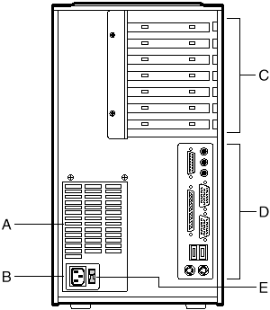
Rear Panel
 |
| A |
Power supply fan vent holes. |
| B |
Socket for AC power cord. |
| C |
Add-in card slots. |
| D |
Typical motherboard I/O connectors. See the motherboard section for
further information. |
| E |
Input voltage selection switch |
 
CMOS
Replacing the configuration battery
A battery on the motherboard keeps the clock and values in CMOS RAM
current when you computer is turned off. The battery should last about seven years. When
the battery begins to die, it loses voltage; when the voltage drops below a certain level,
the Setup program settings stored in CMOS RAM (for example, the date and time) might not
be accurate. Replace the battery with an equivalent one.
Warning
The CMOS battery is a lithium type. Do not use a metal tool to remove the battery. An
accidental short circuit may cause the battery to explode. Dispose of the battery
according to the battery manufacturer's recommendations.
To replace the battery
- Turn off all peripheral devices connected to the computer.
- Turn off the computer and unplug all power cords.
- Take suitable anti-static precautions and remove the computer top and
access covers.
- With your fingers, gently prise the battery free from its socket. Note
the "+" and "-" orientation of the battery.
- Install the new battery in the socket, orienting the "+" and
"-" correctly.
- Replace the computer covers.
 
Motherboard Resources
Memory Map
I/O Map
PCI Configuration Space Map
DMA Channels
Interrupts
Memory Map
| Address Range (decimal) |
Address Range (hex) |
Size |
Description |
| 1024K-393216K |
100000-18000000 |
383MB |
Extended memory |
| 1008K-1024K |
FC000-FFFFF |
16K |
Boot Block |
| 1000K-1008K |
FA000-FBFFF |
8K |
ESCD (Plug and Play configuration and DMI) |
| 996K-1000K |
F9000-F9FFF |
4K |
Reserved for BIOS |
| 992K-996K |
F8000-F8FFF |
4K |
OEM Logo/Scan User Flash |
| 928K-992K |
E8000-F7FFF |
64K |
POST BIOS |
| 896K - 928K |
E0000 - E7FFF |
32K |
POST BIOS (Available as UMB) |
| 800K-896K |
C8000-DFFFF |
96K |
Available high DOS memory (open to ISA and PCI bus) |
| 640K-800K |
A0000-C7FFF |
160K |
Video memory and BIOS |
| 639K-640K |
9FC00-9FFFF |
1K |
Extended BIOS Data (moveable by memory management
software) |
| 512K-639K |
80000-9FBFF |
127K |
Extended conventional memory |
| 0K-512K |
00000-7FFFF |
512K |
Conventional memory |
I/O Map
| Address (hex) |
Size |
Description |
| 0000 - 000F |
16 bytes |
PIIX4 - DMA 1 |
| 0020 - 0021 |
2 bytes |
PIIX4 - Interrupt Controller 1 |
| 002E - 002F |
2 bytes |
SuperI/O Controller Config. Reg. |
| 0040 - 0043 |
4 bytes |
PIIX4 - Timer 1 |
| 0048 - 004B |
4 bytes |
PIIX4 - Timer 2 |
| 0060 |
1 byte |
Keyboard Controller Byte - Reset IRQ |
| 0061 |
1 byte |
PIIX4 - NMI, speaker control |
| 0064 |
1 byte |
Keyboard Controller, CMD/STAT Byte |
| 0070, bit 7 |
1 bit |
PIIX4 - Enable NMI |
| 0070, bits 6:0 |
7 bits |
PIIX4 - Real Time Clock, Address |
| 0071 |
1 byte |
PIIX4 - Real Time Clock, Data |
| 0078 |
1 byte |
Reserved - Brd. Config. |
| 0079 |
1 byte |
Reserved - Brd. Config. |
| 0080 - 008F |
16 bytes |
PIIX4 - DMA Page Registers |
| 00A0 - 00A1 |
2 bytes |
PIIX4 - Interrupt Controller 2 |
| 00B2 - 00B3 |
2 bytes |
APM Control |
| 00C0 - 00DE |
31 bytes |
PIIX4 - DMA 2 |
| 00F0 |
1 byte |
Reset Numeric Error |
| 0170 - 0177 |
8 bytes |
Secondary IDE Channel |
| 01F0 - 01F7 |
8 bytes |
Primary IDE Channel |
| 0201 |
1 byte |
Audio/Game Port |
| 0220 - 022F |
16 bytes |
Audio |
| 0228 - 022F |
8 bytes |
Parallel Port 3 |
| 0240 - 024F |
16 bytes |
Audio |
| 0278 - 027F |
8 bytes |
Parallel Port 2 |
| 0290 - 0297 |
8 bytes |
Management Extension Hardware |
| 02E8 - 02EF |
8 bytes |
Serial Port 4/Video (8514A) |
| 02F8 - 02FF |
8 bytes |
Serial Port 2 |
| 0300 - 0301 |
2 bytes |
MPU-401 (MIDI) |
| 0330 - 0331 |
2 bytes |
MPU-401 (MIDI) |
| 0332 - 0333 |
2 bytes |
MPU-401 (MIDI) |
| 0334 - 0335 |
2 bytes |
MPU-401 (MIDI) |
| 0376 |
1 byte |
Sec. IDE Chan. Cmd. Port |
| 0377 |
1 byte |
Floppy Chan. 2 Cmd. |
| 0377, bit 7 |
1 bit |
Floppy Disk Change, Channel 2 |
| 0377, bits 6:0 |
7 bits |
Sec. IDE Channel Status Port |
| 0378 - 037F |
8 bytes |
Parallel Port 1 |
| 0388 - 038D |
6 bytes |
FM Synthesizer |
| 03B4 - 03B5 |
2 bytes |
VGA |
| 03BA |
1 byte |
VGA |
| 03C0 - 03CA |
11 bytes |
VGA |
| 03CC |
1 byte |
VGA |
| 03CE - 03CF |
2 bytes |
VGA |
| 03D4 - 03D5 |
2 bytes |
VGA |
| 03DA |
1 byte |
VGA |
| 03E8 - 03EF |
8 bytes |
Serial Port 3 |
| 03F0 - 03F5 |
6 bytes |
Floppy Channel 1 |
| 03F6 |
1 byte |
Primary IDE Channel Command Port |
| 03F7 (Write) |
1 byte |
Floppy Channel1 Command |
| 03F7, bit 7 |
1 bit |
Floppy Disk Change Channel 1 |
| 03F7, bits 6:0 |
7 bits |
Primary IDE Channel Status Port |
| 03F8 - 03FF |
8 bytes |
Serial Port 1 |
| 04D0 - 04D1 |
2 bytes |
Edge/level triggered PIC |
| 0530 - 0537 |
8 bytes |
Windows Sound System |
| 0604 - 060B |
8 bytes |
Windows Sound System |
| LPTn + 400h |
8 bytes |
ECP port, LPTn base address + 400h |
| 0CF8 - 0CFB * |
4 bytes |
PCI Configuration Address Register |
| 0CF9 ** |
1 byte |
Turbo & Reset Control Register |
| 0CFC - 0CFF |
4 bytes |
PCI Configuration Data Register |
| 0E80 - 0E87 |
8 bytes |
Windows Sound System |
| 0F40 - 0F47 |
8 bytes |
Windows Sound System |
| 0F86 - 0F87 |
2 bytes |
Yamaha OPL3-SA Configuration |
| FF00 - FF07 |
8 bytes |
IDE Bus Master Register |
| FFA0 - FFA7 |
8 bytes |
Pri. Bus Master IDE Registers |
| FFA8 - FFAF |
8 bytes |
Sec. Bus Master IDE Registers |
* Only by DWORD accesses.
** Only by Byte accesses.
PCI Configuration Space Map
Bus
Number
(hex) |
Device
Number
(hex) |
Function
Number
(hex) |
Description |
00 |
00 |
00 |
Intel 82440LX (PAC) |
00 |
01 |
00 |
Intel 82371AB (PIIX4) AGP Bus |
00 |
07 |
00 |
Intel 82371AB (PIIX4) PCI/ISA Bridge |
00 |
07 |
01 |
Intel 82371AB (PIIX4) IDE Bus Master |
00 |
07 |
02 |
Intel 82371AB (PIIX4) USB |
00 |
07 |
03 |
Intel 82371AB (PIIX4) Power Management |
00 |
0D |
00 |
PCI Expansion Slot 1 (J4D2) |
00 |
0E |
00 |
PCI Expansion Slot 2 (J4D1) |
00 |
0F |
00 |
PCI Expansion Slot 3 (J4C1) |
00 |
10 |
00 |
PCI Expansion Slot 4 (J4B1) |
DMA Channels
| DMA |
Data Width |
System Resource |
0 |
8- or 16-bits |
Audio |
1 |
8- or 16-bits |
Audio if present, else parallel port |
2 |
8- or 16-bits |
Floppy drive |
3 |
8- or 16-bits |
Audio if present, else parallel port (for ECP/EPP configuration) |
4 |
16-bits |
Reserved - Cascade Channel |
5 |
16-bits |
Available |
6 |
16-bits |
Available |
7 |
16-bits |
Available |
Interrupts
IRQ |
System Resource |
NMI |
I/O channel check |
0 |
Reserved, interval timer |
1 |
Reserved, keyboard buffer full |
2 |
Reserved, cascade interrupt from slave PIC |
3 |
Serial Port 2 |
4 |
Serial Port 11 |
5 |
Parallel Port 2 (Plug and Play option) |
6 |
Floppy drive |
7 |
Parallel Port 11 |
8 |
Real-time clock |
9 |
Reserved |
10 |
User available |
11 |
Audio1 if present, else user available |
12 |
Onboard mouse port if present, else user available |
13 |
Reserved, math coprocessor |
14 |
Primary IDE if present, else user available |
15 |
Secondary IDE if present, else user available |
1 Default, but can be changed to another IRQ
 
Beep Codes
The computer uses special audio beep codes to signal certain hardware
faults.
One long beep followed by several short beeps indicates a video problem.
There may be no display on the screen.
| Beeps |
80h Code |
Description |
| 1 |
B4h |
One short beep before boot |
| 1-2 |
98h |
Search for option ROMs |
| 1-2-2-3 |
16h |
BIOS ROM checksum |
| 1-3-1-1 |
20h |
Test DRAM refresh |
| 1-3-1-3 |
22h |
Test keyboard controller |
| 1-3-4-1 |
2Ch |
RAM failure on address line xxxx |
| 1-3-4-3 |
2Eh |
RAM failure on data bits xxxx of low byte of memory bus |
| 1-4-1-1 |
30h |
RAM failure on data bits xxxx of high byte of memory bus |
| 2-1-2-3 |
46h |
Check ROM copyright notice |
| 2-2-3-1 |
58h |
Test for unexpected interrupts |
 

|


