
 |
|
 |
|
 |
 |
Total Memory |
Bank 0 |
Bank 1 |
8 Mb |
8 Mb |
- |
16 Mb |
8 Mb |
8 Mb |
16 Mb |
16 Mb |
- |
24 Mb |
16 Mb |
8 Mb |
32 Mb |
16 Mb |
16 Mb |
32 Mb |
32 Mb |
- |
40 Mb |
32 Mb |
8 Mb |
48 Mb |
32 Mb |
16 Mb |
64 Mb |
32 Mb |
32 Mb |
64 Mb |
64 Mb |
- |
72 Mb |
64 Mb |
|
80 Mb |
64 Mb |
16 Mb |
96 Mb |
64 Mb |
32 Mb |
128 Mb |
64 Mb |
64 Mb |
| 3Com triple-combo (thin/thick/UTP) Ethernet card, (3C509B) | XB55742 |
| 3Com 10/100 PCI Ethernet card (3C595TX) | XB54991 |
| MB | Make | Model | Type | Part Number |
| 545 | Quantum | MV 540 AT | IDE | SU53460 |
| 640 | Quantum | FB 640 AT | IDE | SU56070 |
| 850 | Quantum | TB 850 AT | IDE | SU54941 |
| 1,000 | Quantum | FB 1080 AT | IDE | SU54858 |
| 1,200 | Quantum | FB 1280 AT | IDE | SU55760 |
| 2 GB | IBM | DFHS S2F | SCSI II | SU54096 |
| Tape | ||||
| 400 - 800MB | Conner | CTT800R-F | FDD | SU56352 |
| 4-16GB | Conner | CTD8000R-S | SCSI II | SU54778 |
| 1.6-3.2GB | Conner | CTM3200R-S | SCSI II | XB54027 |
| Floppy | ||||
| Mitsubishi | 355F | 3.5" | ||
| CD-ROM | ||||
| Quad | Sony | CDU76S | SCSI | SU54768 |
| Quad | Sony | CDU77E | IDE | SU56156 |
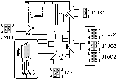
JUMPER |
FUNCTION | PINS JUMPERED |
J7B1 |
Recovery boot enable jumper: If the BIOS is corrupted during an upgrade, this jumper allows you to boot the system and recover the BIOS. | 1 - 2 = Normal (Default) 2 - 3 = Recovery boot enable |
JUMPER |
FUNCTION |
PINS JUMPERED |
J10C2
|
Bus Frequency Multiplier |
2 - 3 4 - 5 1.5 x 1 - 2 4 - 5 2.0 x 1 - 2 5 - 6 2.5 x 1 - 2 4 - 5 Reserved |
J2G1 |
Clock Frequency |
1 - 2 5 - 6 50 MHz 1 - 2 4 - 5 60 MHz 2 - 3 5 - 6 66 MHz 2 - 3 4 - 5 Reserved |
JUMPER |
FUNCTION | PINS JUMPERED |
J10C3 |
Reset CMOS settings to default CMOS RAM values | 2 - 3 = Normal mode (Default) 1 - 2 = Reset CMOS settings |
| Clear password | 5 - 6 = Normal mode (Default) 4 - 5 = Clear password |
JUMPER |
FUNCTION | PINS JUMPERED |
J10C4 |
ISA bus clock speed: Sets the ISA bus to a slower or faster setting. | 2 - 3 = 8.33 MHz (75MHz CPU)(Default) 7.5MHz (90MHz CPU) 8.25MHz (100MHz CPU) 7.5MHz (120MHz CPU) 1 - 2 = 8.33MHz (75MHZ CPU) 10MHz (90MHZ CPU) 11MHz (100MHz CPU) 10MHz (120MHz CPU) |
| Enables/disables access to Setup Progam | 5 - 6 = Setup program can be accessed (Default) 4 - 5 = Setup program access disabled |
JUMPER |
FUNCTION | PINS JUMPERED |
J10K1 |
CPU Voltage Regulator: some upgrade processors may require changing from the default VR setting to the VRE setting | 2 - 3 = VR mode (3.3V - 3.465V)(Default) 1 - 2 = VRE mode (3.465V - 3.63V)
Caution: This jumper should ony be changed to the VRE setting if documentation that came with your upgrade CPU indicates that the required voltage must be between 3.465V and 3.63V. |
| Modems | ||
| Voice/Data modem | XB55987 | |
| Add-in Cards | ||
| SCSI card add-in | SA50160 | |
| Adaptec 2940 PCI SCSI Card | UD55556 | |
| Matrox MGA Millenium PCI, 2MB WRAM | XB57211 | |
| Matrox MGA Millenium PCI, 4MB WRAM | XB57212 | |
| Video RAM | 1MB to 2MB upgrade | XB56217 |
| Cache | 256K Asynch Cache | XB56993 |
| 256K Pipeline Burst Cache | XB56994 |
The on-board S3 Trio64V+ integrated PCI graphics controller is a system component. The S3 controller provides the following features:
Standard 1 MB of graphics memory, expandable to 2 MB
Support for 16-bit bidirectional VESA advanced feature connector
Support for VESA Display Power Management Signaling (DPMS) monitor power saving mode.
Available Resolutions
Pixel Resolution |
Number of Colours |
Refresh Rate (Hz) |
Memory Required |
640 x 480 |
16 |
60 |
1 MB |
640 x 480 |
256 |
60, 72, 75 |
1 MB |
640 x 480 |
32768 |
60, 72, 75 |
1 MB |
640 x 480 |
16.7 million |
60, 72, 75 |
1 MB |
640 x 480 |
4.2 billion |
60, 72, 75 |
2 MB |
800 x 600 |
256 |
56, 60, 72, 75, 85 |
1 MB |
800 x 600 |
32768 |
60, 72, 75 |
1 MB |
800 x 600 |
65536 |
60, 72, 75 |
1 MB |
800 x 600 |
16.7 million |
60, 72, 75 |
2 MB |
800 x 600 |
4.2 billion |
60, 72, 75 |
2 MB |
1024 x 768 |
256 |
43(I), 60, 70, 75, 85 |
1 MB |
1024 x 768 |
32768 |
43(I), 60, 70, 75 |
2 MB |
1024 x 768 |
65536 |
43(I), 60, 70, 75 |
2 MB |
1024 x 768 |
16.7 million |
60, 72, 75 |
2 MB |
1280 x 1024 |
16 |
43(I), 45(I), 60, 72, 75 |
1MB |
1280 x 1024 |
256 |
45(I), 60, 72, 75 |
2 MB |
(I) = Interlaced |
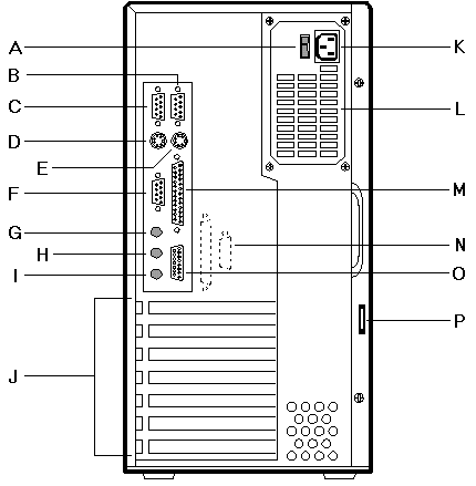
| A - Input voltage select switch | G - Line-in jack | M - Parallel port |
| B - 9-pin Serial Port COM 1 | H - Line-out/Speaker jack | N - Knock outs for I/O ports |
| C - 9-pin Serial Port COM 2 | I - Microphone jack | O - MIDI and dual game port |
| D - PS/2 Mouse/Keyboard | J - Expansion slots | P - Padlock slot |
| E - PS/2 Mouse/Keyboard | K - AC power input | |
| F - Video Connector | L - Power supply fan |
Clear CMOS - Jumper J10C3
Allows CMOS settings to be reset to default values by jumpering pins 1-2 in J10C3. The system should then be turned off and the jumper returned to pins 2-3 to restore normal operation. This procedure should be done whenever the system BIOS is updated.
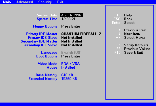
To enter CMOS Setup Press F1 during BOOT.
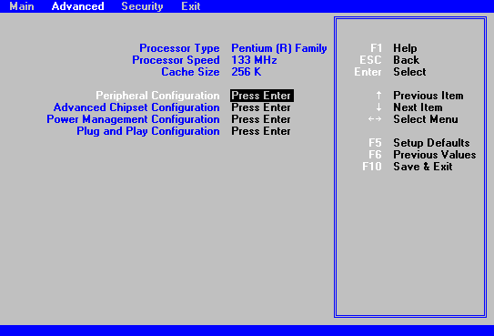
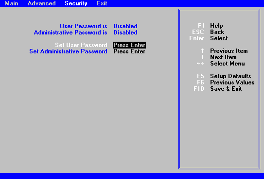
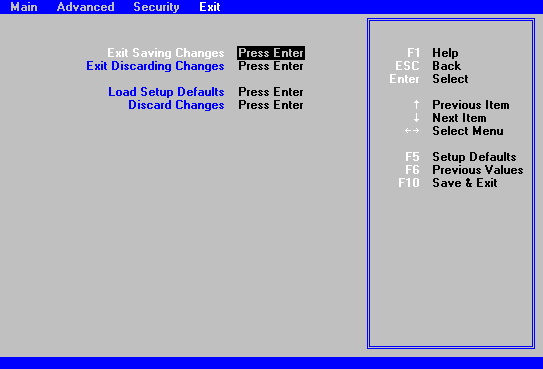
INTERRUPTS, MEMORY and I/O PORTS
Interrupts (IRQ)
Interrupts |
Default Function |
NMI |
I/O Channel Check |
IRQ 0 |
Reserved, Interval Timer |
IRQ 1 |
Reserved, Keyboard buffer full |
IRQ 2 |
Reserved, Cascade interrupt |
IRQ 3 |
Serial port 2 |
IRQ 4 |
Serial port 1 |
IRQ 5 |
User available |
IRQ 6 |
Floppy |
IRQ 7 |
Parallel port 1 |
IRQ 8 |
Real time clock |
IRQ 9 |
User available |
IRQ 10 |
User available |
IRQ 11 |
User available |
IRQ 12 |
On-board Mouse port |
IRQ 13 |
Reserved, Math co processor |
IRQ 14 |
Primary ATA/IDE interface |
IRQ 15 |
Secondary ATA/IDE interface |
Memory Map
Address Range (Decimal) |
Address Range (Hex.) |
Size |
Description |
1024K-131072K |
100000-8000000 |
127M |
Extended Memory |
960K-1023K |
F0000-FFFFF |
64K |
AMI System BIOS |
952K-959K |
EE000-EFFFF |
8K |
FLASH Boot Block (Available as UMB) |
948K-951K |
ED000-EDFFF |
4K |
ECSD (Plug and Play configuration area) |
944K-947K |
EC000-ECFFF |
4K |
OEM LOGO (available as UMB) |
896K-943K |
E0000-EBFFF |
48K |
BIOS RESERVED (Currently available as UMB) |
800K-895K |
C8000-DFFFF |
96K |
Available HI DOS memory (open to ISA and PCI bus) |
640K-799K |
A0000-C7FFF |
160K |
Video Memory and BIOS |
I/O Ports
I/O ports (Hex) |
Used by |
000 - 00F |
DMA controller 1 |
020 - 021 |
Interrupt controller 1 |
02E - 02F |
Ultea I/O configuration registers |
040 - 043 |
Timer 1 |
048 - 04B |
Timer 2 |
060 |
Keyboard controller data byte |
061 |
NMI, speaker control |
064 |
Keyboard controller, CMD/STAT Byte |
070 bit 7 |
Enable NMI |
070 bits 6:0 |
Real Time Clock, Address |
071 |
Real Time Clock, Data |
078 |
Reserved - Brd config |
079 |
Reserved - Brd config |
080 - 08F |
DMA Page Register |
0A0 - 0A1 |
Interrupt Controller 2 |
0C0 - 0DE |
DMA 2 |
0F0 |
Reset Numeric Error |
170 - 177 |
Secondary IDE Channel |
1F0 - 1F7 |
Primary IDE Channel |
278 - 27B |
Parallel Port 2 |
2F8 - 2FF |
On-Board Serial Port 2 |
376 |
Second IDE Channel Command Port |
377 |
Second IDE Channel Stat Port |
378 - 37F |
Parallel Port 1 |
3BC - 3BF |
Parallel Port x |
3E8 - 3EF |
Serial port 3 |
3F0 - 3F5 |
Floppy Channel 1 |
3F6 |
Primary IDE Channel Command Port |
3F7 (Write) |
Floppy Channel 1 Command |
3F7, bit 7 |
Floppy Disk Change Channel 1 |
3F7, bits 6:0 |
Primary IDE Channel Status Port |
3F8 - 3FF |
On-Board Serial Port 1 |
LPT + 400 |
ECP port, LPT + 400 |
4D0 - 4D1 |
Edge/Level INTR Control Register |
Direct memory access (DMA) channel
DMA |
Data Width |
System Resource |
DMA 0 |
8 or 16 bits |
Open |
DMA 1 |
8 or 16 bits |
Open |
DMA 2 |
8 or 16 bits |
Diskette Controller |
DMA 3 |
8 or 16 bits |
Parallel Port (ECP/EPP) |
DMA 4 |
System | |
DMA 5 |
16 bits |
Open |
DMA 6 |
16 bits |
Open |
DMA 7 |
16 bits |
Open |
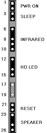
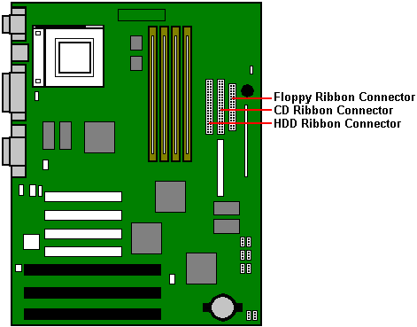
Other Motherboard Conections
![]()