 |


|
|
FT2400 'Nexus' Madrona
Motherboard Layout
 
Front & Rear Views
Font View
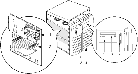
|
| 1 |
Processor sockets |
5 |
Full-width peripheral bays |
| 2 |
Memory board |
6 |
CD-ROM drive |
| 3 |
Control panel & indicators |
7 |
Floppy diskette drive |
| 4 |
SCSI hot-docking bays |
|
Rear View
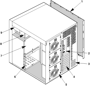
|
1 |
Left side cover |
6 |
SCSI hot-docking bay |
2 |
I/O panel |
7 |
SCSI hot-docking backplane |
3 |
Knock-out slots for external SCSI connectors |
8 |
Half-height peripheral bays |
4 |
Expansion slots |
9 |
Floppy diskette drive (vertical) |
5 |
Power supplies |
|

|
1 |
PS/2 keyboard port, 6-pin connector |
4 |
Parallel port (LPT), 25-pin connector |
2 |
PS/2 mouse port, 6-pin connector |
5 |
SVGA, 15-pin video connector |
3 |
Serial port 1 (COM1), 9-pin connector |
6 |
Serial port 2 (COM2), 9-pin connector |
 
Motherboard
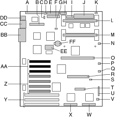
|
| A |
Narrow SCSI connector |
Q |
Fan 3 connector |
| B |
IDE connector |
R |
RPX connector (option) |
| C |
I2C connector |
S |
I2C connector |
| D |
Fan 0 |
T |
Server management connector |
| E |
Floppy drive connector |
U |
Jumper block J2J1 |
| F |
Power connector |
V |
Fan 4 connector |
| G |
Hard disk activity input |
W |
Wide SCSI channel B |
| H |
Auxillary power connector |
X |
Wide SCSI channel A |
| I |
Front panel connector |
Y |
ISA bus slots |
| J |
VRM connector |
Z |
Secondary PCI slots |
| K |
Speaker connector |
AA |
Primary PCI slots |
| L |
Secondary processor connector |
BB |
Parallel and Video connectors |
| M |
Primary processor connector |
CC |
Serial port 1 and Serial port 2 connectors |
| N |
Blower 1 connector |
DD |
Keyboard and mouse connectors |
| O |
Memory module connector |
EE |
Video memory upgrade socket |
| P |
Blower 2 connector |
FF |
Back-up battery |
 
Processor Upgrade
In a symmetric multiprocessor (SMP) environment all processors are equal
and have no preassigned tasks. Distributing the processing loads between both processors
increases system performance. This is particularly useful when application demand is low
and the I/O request load is high. In an SMP environment, both processors share a common
bus, the same interrupt structure, and access to common memory and I/O channels. The SMP
implementation conforms to the Multiprocessor Specification Version 1.4.
If the supplied system is fitted with only a single processor, a second
processor and DC converter (VRM) may be fitted. The second processor must be identical to
the one already installed. The second processor slot, if unused must have a
termination board fitted.
Removing the Termination Board
Do not remove this board unless you are adding a second processor.
- Remove the left side cover.
- Press the latches on the Terminator Latching Assembly (TLA) inward.
- Pull the TLA out of the module retention bracket.
- Holding the terminator board by its top edge, carefully rock it back and
forth until the edge connector pulls free.
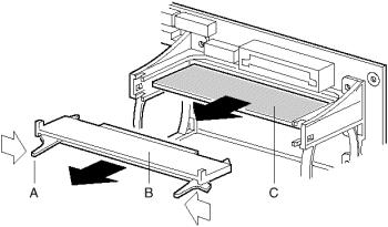
|
| A |
Latch |
| B |
Terminator Latching Assembly |
| C |
Terminator Board |
Installing a Voltage Regulator Module
- Remove the left side cover.
- Being careful not to touch the components or connector on the voltage
regulator module, remove it from its protective wrapper and place it on a nonconductive,
static-free surface.
- Record the module ID information (may be a date code) in your equipment
log.
- Hold the module by its top edge or upper corners and firmly press it into
the connector on the system board until the lock tabs click into place.

|
| 1 |
Module |
| 2 |
Connector |
| 3 |
Lock Tab |
Installing a second Pentium II Processor
- Remove the left side cover.
- Remove the termination board as previously described.
- Fit the VRM as previously described.
- Being careful not to touch the components or gold edge connectors on the
processor module, remove it from its protective wrapper and place it heat-sink side down
on a nonconductive, static-free surface.
- Record the module serial number in your equipment log.
- Press the locking tabs inward until they remain retracted.
- Hold the module by its top edge or upper corners, and firmly press it
into the connector on the system board. Press the locking tabs outward so they engage the
support bracket.

- Replace the left side cover.
- Run the SCU to configure the system.
 
Memory Module
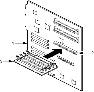
The SDRAM memory module is a motherboard sub-board which plugs into a
slot on the system board as shown in the diagram below:
|
| 1 |
System board |
| 2 |
Connector |
| 3 |
Memory Module |
The SDRAM memory module has four DIMM sockets. This
module supports from 16 MB to 512 MB of 3.3V, 66 MHz, unbuffered, 72-bit
ECC SDRAM modules. Mixing dissimilar metals may cause failure. Install DIMMs with
gold-lead alloy plated edge connectors only in gold-lead alloy plated sockets.
It is recommended that all DIMMs should be of the same size, type and
speed. Although it is possible to mix different DIMM sizes, mixes of type and speed can be
problematic. Only type and speed mixes which have been positively cleared by Mitsubishi
Electric for factory build can be used. The BIOS automatically detects and initialises the
memory array.
ECC memory detects and corrects single-bit errors from DRAM in real
time, allowing your system to function normally. It detects all double-bit errors but does
not correct them; it also detects all three-bit and four-bit adjacent errors in a DRAM
nibble but does not correct them. When one of these multiple-bit errors occurs, the PAC
generates an SERR (system error) that usually halts the system. ECC is calculated on a
64-bit wide memory basis.
To avoid potential memory problems, use only DIMMs from JEDEC-compatible
manufacturers that have been tested for compatibility with the memory module. Contact your
sales representative or dealer for a list of approved DIMMs.
Sample DIMM Size Combinations - SDRAM module
Banks Filled |
0, J1 |
1, J2 |
2, J3 |
3, J4 |
Total Memory |
16 |
16 |
|
|
32 MB |
16 |
16 |
16 |
|
48 MB |
32 |
32 |
32 |
|
96 MB |
32 |
32 |
32 |
32 |
128 MB |
64 |
64 |
64 |
64 |
256 MB |
128 |
128 |
128 |
128 |
512 MB |
 
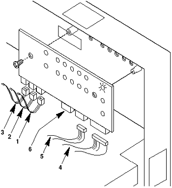
Front Panel Board
|
| 1 |
J1, alarm switch cable for access doors to hot-docking bays |
| 2 |
J2, alarm switch cable for right side panel |
| 3 |
J3, alarm switch cable for left side panel |
| 4 |
J4, system board control signal cable |
| 5 |
J5, top SCSI hot-docking backplane cable |
| 6 |
J6, connector for the bottom SCSI hot-docking backplane cable |
 
Hot-docking Backplane
The chassis contains provision for 2 off 5 slot hot-docking backplanes.
The hot-docking backplane provides the following:
- Five SCA connectors for SCA-compatible SCSI drives
- Power control for each drive, including automatic slot power down upon
removing a drive
- Signal for a fault indicaton (LED) on the front panel for each drive
- Internal I2C bus
- +12 V connector for a fan with tachometer
- Local I2C-based temperature sensor
The SCSI hot-docking backplane provides control signals and power for
five wide/fast SCA SCSI III hard disk drives. The backplane receives control signals from
the Symbios SCSI controller on the system board through a cable connected to the wide SCSI
connector on the backplane. It gets power from the power system through 4-conductor cables
connected to the two power connectors.
The SCSI hard disk drives in the hot-docking bay get their control
signals and power from the SCA connectors on the hot-docking backplane.
The fault indicators (LEDs) on the front panel indicate failure status
for each drive in the hot-docking bay. These indicators get their signals through a cable
connected to the front panel connector on the hot-docking backplane.
The temperature sensor on the backplane provides temperature information
to other devices in the server through enclosure service messages.
The backplane power control provides powering down of a drive when a
failure is detected and reported to the SCSI bus through enclosure service messages. When
a new drive is inserted in the hot-docking SCA connector, the power control waits a short
time for the drive to become fully seated and then applies power to the drive.
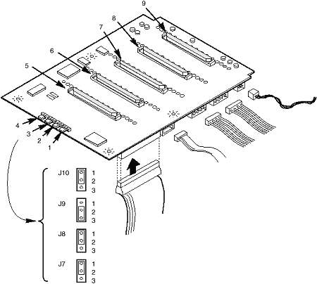
|
1 |
SCSI ID B, J10 |
6 |
SCSI drive 3 |
2 |
SCSI ID A, J9 |
7 |
SCSI drive 2 |
3 |
Internal/external, J8 |
8 |
SCSI drive 1 |
4 |
Normal operation, J7 |
9 |
SCSI drive 0 |
5 |
SCSI drive 4 |
|
|
Configuration Options
The hot-docking backplane contains only one configuration jumper: J8,
the internal/external jumper.
Internal/External (INT/EXT) Jumper J8
When this jumper is in the "INT" position, jumper on pins 1
and 2, (default setting) the backplane assumes it is operating in an "internal"
peripheral bay in the server chassis.
When this jumper is in the "EXT" position, jumper on pins 2
and 3, the backplane assumes it is operating in an "external" peripheral bay in
a peripheral expansion chassis. This option is not currently available with this
computer and must not be selected.
SCSI ID Configuration Options
The SCSI chip on the hot-docking backplane uses the SAF-TE protocol to
communicate with the system board. This chip uses SCSI ID 6; therefore, other SCSI devices
cannot use this address.
J10 |
J9 |
Drive 0 |
Drive 1 |
Drive 2 |
Drive 3 |
Drive 4 |
2-3 |
2-3 |
ID8 |
ID9 |
ID2 |
ID11 |
ID12 |
1-2 * |
2-3 * |
ID0 |
ID1 |
ID2 |
ID3 |
ID4 |
2-3 |
1-2 |
ID8 |
ID9 |
ID10 |
ID11 |
ID12 |
1-2 |
1-2 |
ID0 |
ID1 |
ID10 |
ID3 |
ID4 |
* Jumper default setting.
 
Power Distribution
Power Share Backplane
The power share backplane distributes the power load of the server among
two or three power supplies. The backplane is mounted on two snap-on stand-offs and six
threaded stand-offs on the centre wall inside the chassis.
Warning
Hazardous voltage, current, and energy levels are present inside the power share
backplane. There are no user serviceable parts inside it; servicing should only be done by
technically qualified personnel.
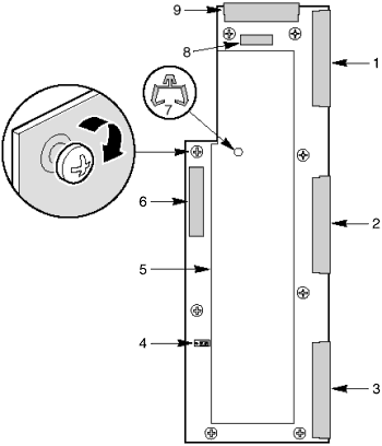
|
1 |
Top power supply connector |
6 |
Output to system peripherals |
2 |
Centre power supply connector |
7 |
PSU fan cable support clip |
3 |
Lower power supply connector |
8 |
Aux power out to motherboard |
4 |
Factory configured jumper (reserved) |
9 |
Main output to motherboard |
5 |
Non-removable screen/cover |
Power System Configurations
The server contaions a modular power system that may be configured with
one, two, or three 360 Watt power supplies.
| Configuration level |
Redundancy |
Number of supplies |
| Entry |
Non-redundant |
1 |
| Entry |
Redundant |
2 |
| Maximum |
Non-redundant |
2 |
| Maximum |
Redundant |
3 |
An entry level power system typically limits the server
configuration to dual processors, 1 GB memory, five hard drives, and total power
dissipated. A maximum level power system provides power for fully configured servers.
Each power supply has a built-in fan and its own power cord. For servers
with redundant power systems, the loss of a single power supply will not affect the
operation of the server.
| Power System Voltages |
+3.3V |
+5V |
+12V |
-5V |
-12V |
| One power supply, entry level non-redundant (total
combined output power of +3.3V and +5V should not exceed 178W) |
13A |
32A |
15.5A |
0.25A |
0.5A |
| Two power supplies, entry level redundant |
13A* |
30A |
13.5A |
0.25A |
0.5A |
| Two power supplies, maximum level non-redundant |
18A** |
46A |
29A |
0.5A |
1.0A |
| Three power supplies, maximum level redundant |
18A** |
46A |
29A |
0.5A |
1.0A |
* No more than 5A to be used by PCI slots
** No more than 10A to be used by PCI slots |
 
Drives & Add-Ins
| Hard Drives |
| MB |
Make |
Model |
Type |
Part Number |
| 4.5GB |
Quantum |
HN4550J 'Atlas
II' |
UltraSCSI |
HB58476 |
| 9GB |
IBM |
DDRS-39130
'Draco' |
UltraSCSI |
XB62206 |
|
| Tape Drive |
| MB |
Make |
Model |
Type |
Part Number |
| 12-24GB |
HP |
HP
C1537A |
DDS III |
SU61220 |
| 72-144GB |
HP |
HP
C1557A Autoloader |
DDS III |
SU61226 |
|
| Floppy Drives |
| MB |
Type |
Part Number |
|
|
| 2 MB |
3.5" |
16284630 |
|
|
|
| CD-ROM |
| Speed |
Type |
Part Number |
|
|
| 16x |
IDE |
16285530 |
|
|
Add-ins
| DIMM memory expansion |
|
| 32MB upgrade (1 x 32MB SDRAM DIMM) |
XB62607 |
| 64MB upgrade (1 x 64MB SDRAM DIMM) |
XB62608 |
| 128MB upgrade (1 x 128MB SDRAM DIMM) |
XB62609 |
| Additional Processors |
|
| Single to dual Pentium II at 300MHz, 512KByte Cache |
XB62828 |
| Redundant Power Supply |
|
| N+1 Redundant power supply upgrade (includes 1 PSU modules) |
XB6000 |
| Additional hot swap power supply module for the above |
XB62296 |
| Network options |
|
| 3Com 10/100 PCI Ethernet card (3C905TX) |
XB59527 |
| 3Com PCI Ethernet Combo card (3C900) |
XB59526 |
| Intel Pro 100B PCI Ethernet Card |
XB61343 |
| Rack Mount Kit |
|
| Rack mount assembly for mounting server in 19" rack |
XB61584 |
| Controller cards |
|
| 2nd backplane for additional U/W SCSI channel |
XB62320 |
| RAID |
|
| AMI 434 2 channel RAID (requires 2nd backplane for dual channel) |
XB6001 |
| 4MB AMI RAID Cache Upgrade |
XB61650 |
| Server Management |
|
| Server Management Card |
XB61339 |
| Modem for the above (PCMCIA) |
XB61341 |
| UPS |
|
| APC 1000v/a Smart UPS |
XB60370 |
 
Jumper Settings
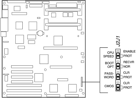
|
| Jumper |
Pins
(default in bold) |
Description |
| CPU Speed |
Enable |
Permits changing the processor speed in the BIOS Setup program. |
| Protect |
Prevents changing the processor speed. |
| Boot Option |
Recovery Boot |
Prevents inverting address A16. Allows the system to boot from the
Recovery BIOS when the normal BIOS gets corrupted if you are unable to reload a fresh copy
from the diskette. |
| Normal Boot |
Inverts address A16 so the Normal BIOS does not reside at the top of
Flash memory where the write-protected Recovery BIOS region is located. |
| Password |
Clear |
Clears the password. |
| Protect |
Maintains the current system password. |
| CMOS |
Clear |
Replaces the contents of NVRAM with the manufacturing default settings. |
| Protect |
Preserves the contents of NVRAM. |
 
CMOS
The jumper on the J2J1, CMOS PROT pins preserves the CMOS settings
during system reset. Moving the jumper to the CLR pins clears CMOS and sets it and the
real-time clock (RTC) to the manufacturing default settings during system reset.
To reset the system’s CMOS and the RTC to factory default values:
- Remove the left side cover.
- Move the jumper on the J2J1, CMOS PROT pins to the CLR pins.
- Replace the left side cover, and connect the power cord(s) to the system.
- Turn the system on, and wait for POST to complete. This automatically
reprograms CMOS and RTC to their default settings.
- Turn the system off, disconnect the power cord(s) from the system, and
remove the left side cover.
- Move the jumper on the J2J1, CMOS CLR pins to the PROT pins.
- Replace the left side cover, and connect the power cord(s) to the system.
- Run the SCU to configure your system.
Back-up Battery
The lithium battery on the system board powers the real-time clock (RTC)
for up to 10 years in the absence of power. The RTC contains 256 bytes of general purpose
RAM that stores the system BIOS configuration information, clock registers, and general
purpose control registers. When the battery starts to weaken, it loses voltage, and the
system settings stored in CMOS RAM in the RTC (for example, the date and time) may be
wrong.
Replacing the Back-up Battery
- Remove the left side cover.
- Locate the battery from the diagram of the motherboard,
where it is identified as ‘FF’.
- Insert the tip of a small plastic tool, or equivalent, under the plastic
tab on the snap-on plastic retainer. Gently lift up and pull back on the retainer to
remove it from the lithium battery socket.
Warning
Do not use a metal or other conductive implement to remove the battery.
If a short-circuit is accidentally made between its positive and negative terminals, it
may cause the battery to explode.
- Remove the battery from its socket.
- Dispose of the old lithium battery according to the battery
manufacter’s instructions.
- Remove the new lithium battery from its package, and, being careful to
observe the correct polarity, insert it into the battery socket.
- Install the snap-on plastic retainer on the socket and make sure it holds
the battery firmly.
- Replace the left side cover.
- Run the SCU to restore the configuration settings to the RTC.
 
System Resources
I/O Map
The I/O map in the following table shows the location in I/O space of
all directly I/O accessible registers.
| Address |
Resource |
| 0000h–000Fh |
DMA Controller 1 |
| 0020h–0021h |
Interrupt Controller 1 |
| 002Eh–002Fh |
Super I/O Index and Data Ports |
| 0040h–0043h |
Programmable Timer |
| 0060h, 0064h |
Keyboard Controller |
| 0061h |
NMI Status & Control Register |
| 0070h |
NMI Mask (bit 7) & RTC Address (bits 6:0) |
| 0071h |
Real Time Clock (RTC) |
| 0080h–0081h |
BIOS Timer |
| 0080h–008Fh |
DMA Low Page Register |
| 0092h |
System Control Port A (PC-AT † control Port) |
| 00A0h–00BFh |
Interrupt Controller 2 |
| 00C0h–00DFh |
DMA Controller 2 |
| 00F0h |
Clear NPX error |
| 00F8h–00FFh |
x87 Numeric Coprocessor |
| 0170h–0177h |
Secondary Fixed Disk Controller (IDE) |
| 01F0h–01F7h |
Primary Fixed Disk Controller (IDE) |
| 0200h–0207h |
Game I/O Port |
| 0220h–022Fh |
Serial Port A |
| 0238h–023Fh |
Serial Port B |
| 0278h–027Fh |
Parallel Port 3 |
| 02E8h–02EFh |
Serial Port B |
| 02F8h–02FFh |
Serial Port B |
| 0338h–033Fh |
Serial Port B |
| 0370h–0375h |
Secondary Floppy |
| 0378h–037Fh |
Parallel Port 2 |
| 03B4h–03BAh |
Monochrome Display Port |
| 03BCh–03BFh |
Parallel Port 1 (Primary) |
| 03C0h–03CFh |
Video Display Controller |
| 03D4h–03DAh |
Color Graphics Controller |
| 03E8h–03EFh |
Serial Port A |
| 03F0h–03F5h |
Floppy Disk Controller |
| 03F6h–03F7h |
Primary IDE - Secondary Floppy |
| 03F8h–03FFh |
Serial Port A (Primary) |
| 0400h–043Fh |
DMA Controller 1, Extended Mode Registers |
| 0461h |
Extended NMI / Reset Control |
| 0462h |
Software NMI |
| 0480h–048Fh |
DMA High Page Register |
| 04C0h–04CFh |
DMA Controller 2, High Base Register |
| 04D0h–04D1h |
Interrupt Controllers 1 and 2 Control Register |
| 04D4h–04D7h |
DMA Controller 2, Extended Mode Register |
| 04D8h–04DFh |
Reserved |
| 04E0h–04FFh |
DMA Channel Stop Registers |
| 0678h–067Ah |
Parallel Port (ECP) |
| 0778h–077Ah |
Parallel Port (ECP) |
| 07BCh–07BEh |
Parallel Port (ECP) |
| 0800h–08FFh |
NVRAM |
| 0CA4 |
PCI to IRQ rerouter control (PCI_INTB_L, PCI_INTA_L) |
| 0CA5 |
PCI to IRQ rerouter control (PCI_INTD_L, PCI_INTC_L) |
| 0CA6h–0CA7h |
Reserved |
| 0CA9h |
DISMIC Data Register |
| 0CAAh |
DISMIC Control/Status Register |
| 0CABh |
DISMIC Flags Register |
| 0C84h |
Board Revision Register |
| 0C85h–0C86h |
BIOS Function Control |
| 0CF8h |
PCI CONFIG_ADDRESS Register |
| 0CF9h |
PMC Turbo and Reset control |
| 0CFCh |
PCI CONFIG_DATA Register |
| 46E8h |
Video Display Controller |
| xx00–xx1F* |
SCSI registers |
* SCSI I/O base address is set using the configuration registers.
Interrupts
The following table shows the logical interrupt mapping of interrupt
sources on the system board.
| Interrupt |
Description
(active-low signals have an "_L" symbol following them) |
| INTR |
Processor interrupt. |
| NMI |
NMI from DISMIC to processor. |
| IRQ0/MIRQ0 |
System board interrupt request 0 connected to input 2 of
the I/O Apic. (For proper operation, the BIOS must set the IRQ0 enable bit in PIIX3
register 70h during initialization.) |
| IRQ1 |
RTC. |
| IRQ3 |
Serial port A or B interrupt from 87307VUL device, user
configurable. |
| IRQ4 |
Serial port A or B interrupt from 87307VUL device, user
configurable. |
| IRQ5 |
Parallel port. |
| IRQ6 |
Floppy diskette. |
| IRQ7 |
Parallel port. |
| IRQ8_L |
|
| IRQ9 |
|
| IRQ10 |
|
| IRQ11 |
|
| IRQ12 |
Keyboard/mouse interrupt from 87307VUL. |
| IRQ14 |
Compatibility IDE interrupt from primary IDE devices 0
and 1. |
| IRQ15 |
|
| IDE_IRQ |
Tied to IRQ14; hard wired from PIIX3. |
The following signals will be rerouted to the above interrupts: |
| PCI_INTA_L |
PCI Interrupt signal A from PIIX3. Wired to PCI-0 slot 1
INTA_L, PCI-0 slot 2 INTD_L, PCI-0 slot 3 INTC_L, PCI-0 slot 4 INTB_L, PCI-1 slot 1
INTA_L, and PCI-1 slot 2 INTD_L. |
| PCI_INTB_L |
PCI Interrupt signal B from PIIX3. Wired to PCI-0 slot 1
INTB_L, PCI-0 slot 2 INTA_L, PCI-0 slot 3 INTD_L, PCI-0 slot 4 INTC_L, PCI-1 slot 1
INTB_L, and PCI-1 slot 2 INTA_L. This interrupt is also used by the SCSI controller. |
| PCI_INTC_L |
PCI Interrupt signal C from PIIX3. Wired to PCI-0 slot 1
INTC_L, PCI-0 slot 2 INTB_L, PCI-0 slot 3 INTA_L, PCI-0 slot 4 INTD_L, PCI-1 slot 1
INTC_L, and PCI-1 slot 2 INTB_L. This interrupt is also used by the Network controller. |
| PCI_INTD_L |
PCI Interrupt signal D from PIIX3. Wired to PCI-0 slot 1
INTD_L, PCI-0 slot 2 INTC_L, PCI-0 slot 3 INTB_L, PCI-0 slot 4 INTA_L, PCI-1 slot 1
INTD_L, PCI-1 slot 2 INTC_L. SMI_L System Management Interrupt. General-purpose error
indicator from a control PAL that provides an SMI_L from nontraditional error sources
(PERR_L, SERR_L, and others). |
 
POST Beep Codes
POST cannot display messages when an error occurs before the video
display is initialised. Instead, it emits one long and two short beeps. Other
beep codes are a series of individual beeps, each one equal in length. Write down the beep
code you hear, plus any error messages that appear; this information will assist in fault
diagnosis.
| Beeps |
Error Message and Conditions |
| 1-2 |
ROM checksum error; ROM checksum does not match encoded value in BIOS. |
| 1-2-2-3 |
ROM checksum error; ROM checksum does not match encoded value in BIOS. |
| 1-3-1-1 |
Refresh failure; memory refresh circuitry on the baseboard is faulty. |
| 1-3-1-3 |
Keyboard controller gate A20 is off; BIOS cannot switch to protected
mode. |
| 1-3-4-1 |
Memory error. |
| 1-4-1-1 |
Memory error. |
| 2-1-2-3 |
ROM copyright notice failure. |
| 2-2-3-1 |
Unexpected interrupt. |
 

|


