 |


|
|
FT2400 'Plexus' Buckeye
Motherboard Layout (Rev 1.14)
 
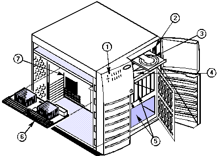
Front View
|
| 1 |
Front panel |
5 |
SCSI hot-docking bays |
| 2 |
Floppy diskette drive |
6 |
Dual Pentium Pro processor/memory module |
| 3 |
CD-ROM drive |
7 |
System board |
| 4 |
5.25-inch external bays |
|
|
 
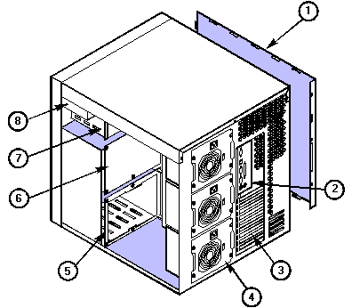
Rear View
|
1 |
Left side cover |
5 |
SCSI hot-docking bay |
2 |
I/O panel |
6 |
SCSI hot-docking backplane |
3 |
Expansion slots |
7 |
Half-height peripheral bays |
4 |
Power supplies |
8 |
Floppy diskette drive (vertical) |

|
1 |
Serial port 2 (COM2), 9-pin connector |
5 |
SVGA, 15-pin video connector |
2 |
Parallel port (LPT), 25-pin connector |
6 |
Serial port 1 (COM1), 9-pin connector |
3 |
PS/2 mouse port, 6-pin connector |
7 |
RJ45 Network controller port |
4 |
PS/2 keyboard port, 6-pin connector |
|
|
 
Motherboard
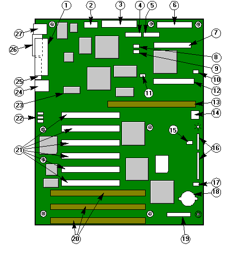 |
| 1 |
Parallel port (LPT) |
15 |
HDD activity - J40 |
| 2 |
Ribbon connector for COM2 |
16 |
Jumpers/options |
| 3 |
Power |
17 |
Fan 2, bottom front |
| 4 |
Auxiliary power |
18 |
CMOS battery |
| 5 |
Front panel |
19 |
Server management port |
| 6 |
Floppy drive port |
20 |
ISA bus card slots |
| 7 |
SCSI |
21 |
PCI bus card slots |
| 8 |
Fan 1, primary roof |
22 |
Network status LEDs |
| 9 |
Fan 3, secondary roof |
23 |
Video memory upgrade |
| 10 |
Fan 4, middle roof |
24 |
Keyboard and mouse ports |
| 11 |
I2C - J45 |
25 |
Video |
| 12 |
IDE |
26 |
Serial port (COM1) |
| 13 |
Processor/Memory board socket |
27 |
Ethernet port |
| 14 |
Speaker |
|
 
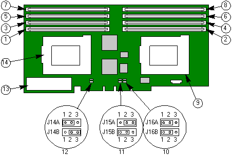
Processor and Memory Module
|
1 |
Bank 0, J1 |
8 |
Bank 7, J8 |
2 |
Bank 1, J2 |
9 |
Primary Pentium Pro processor 0, U10 |
3 |
Bank 2, J3 |
10 |
Jumper block, J16 (A and B) |
4 |
Bank 3, J4 |
11 |
Jumper block, J15 (A and B) |
5 |
Bank 4, J5 |
12 |
Jumper block, J14 (A and B) |
6 |
Bank 5, J6 |
13 |
VRM 12V input, J9 |
7 |
Bank 6, J7 |
14 |
Secondary Pentium Pro processor 1, U7 |
| Processor/Bus Speed |
J14A CLKSEL 1 |
J14B CLKSEL 0 |
J15A CLKDIV 2 |
J15B CLKDIV 1 |
J16A CLKDIV 0 |
150/60 |
1-2 |
2-3 |
2-3 |
1-2 |
1-2 |
166/66 |
2-3 |
1-2 |
2-3 |
1-2 |
1-2 |
180/60 |
1-2 |
2-3 |
1-2 |
2-3 |
1-2 |
200/66 |
2-3 |
1-2 |
1-2 |
2-3 |
1-2 |
| J16B, Reserved |
| 1-2 |
ITP Reserved |
| 2-3* |
Normal operation |
Memory
The memory is configured from 8 DIMM sockets supporting ECC. A single
DIMM socket is a single memory bank. Memory banks can be populated with any size of DIMM,
banks should be filled in ascending order. Single bit error correction and multi bit error
detection is done by the memory controller. DIMM types 32MB, 64MB, and 128MB DIMMS are
supported. Memory is detected automatically from the BIOS , no jumpers are required.
Maximum system memory is therefore 2GB.
Note: Micron 256MB DIMMS do not fit within the chassis ,
suggested limitation to 128MB DIMMS.
Sample DIMM size configurations
Banks Filled |
|
0, J1 |
1, J2 |
2, J3 |
3, J4 |
4, J5 |
5, J6 |
6, J7 |
7, J8 |
Total Memory |
32 |
|
|
|
|
|
|
|
32 MB |
32 |
64 |
64 |
128 |
128 |
|
|
|
416 MB |
64 |
64 |
32 |
32 |
128 |
128 |
|
|
448 MB |
128 |
128 |
128 |
128 |
128 |
128 |
128 |
128 |
1024 MB |
 
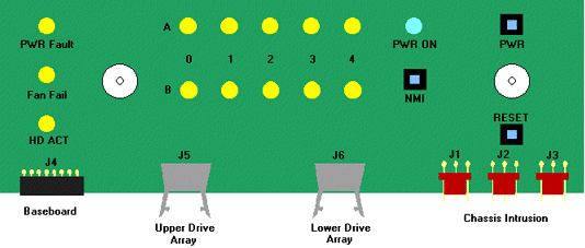
Front Panel Controller
 
Hot Swap Backplane
The chassis contains provision for 2 off 5 slot hot swap backplanes.
These can support only 1inch high SCA II drives. The backplanes can support up to Ultra
Wide data transfers of 40Mb/sec. On each backplane is a SAF-TE / I2C
controller. This allows the system to detect drive insertions and removals as they happen
to the system. Control of the system is primarily through the I2C
bus . LED control is also achieved through the I2C bus and
microcontroller. The controller needs to be initialised to drive the front panel. The
SAF-TE target is always set to SCSI ID 6.
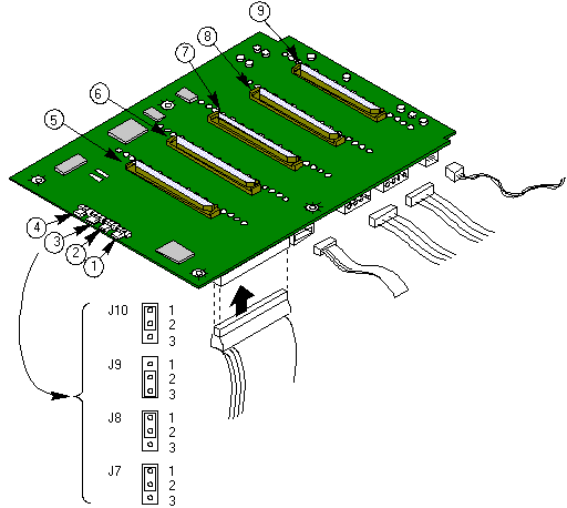
|
1 |
SCSI ID B, J10 |
6 |
SCSI drive 3 |
2 |
SCSI ID A, J9 |
7 |
SCSI drive 2 |
3 |
Internal/external, J8 |
8 |
SCSI drive 1 |
4 |
Normal operation, J7 |
9 |
SCSI drive 0 |
5 |
SCSI drive 4 |
|
|
Jumper Options
| Jumper |
Pins (default in bold) |
|
| J7 Normal/Force Update |
1:2 - Normal
2:3 - Force Update |
|
| J8 Int/Ext |
1:2 - Internal Operation
2:3 - External configuration |
Tells the backplane that it is inside or outside the
chassis , internal is only option supported. |
The drive ID’s are set by the backplane according to
the settings of the J9 and J10 jumpers and the following table.
| J9 |
J10 |
Drive 1 |
Drive 2 |
Drive 3 |
Drive 4 |
Drive 5 |
| 2:3 |
2:3 |
ID 8 |
ID 9 |
ID 2 |
ID 11 |
ID 12 |
| 1:2 |
2:3 |
ID 0 |
ID 1 |
ID 2 |
ID 3 |
ID 4 |
| 2:3 |
1:2 |
ID 8 |
ID 9 |
ID 10 |
ID 11 |
ID 12 |
| 1:2 |
1:2 |
ID 0 |
ID 1 |
ID 10 |
ID 3 |
ID 4 |
SCSI BIOS’s should be set to spin up drives as the
backplane does not implement this function.
The SAF-TE target should support the following notifications
PSU failures - only if the load sharing backplane is installed
Fan Failures
Drive removals and insertions - only if AMI card fitted.
Note that it is the responsibility of the SAF-TE device to spin
up drives during operation of the system.
Note installation of second backplane requires power and
control cables to be connected to the PSU and front panel board respectively.
 
Power Distribution
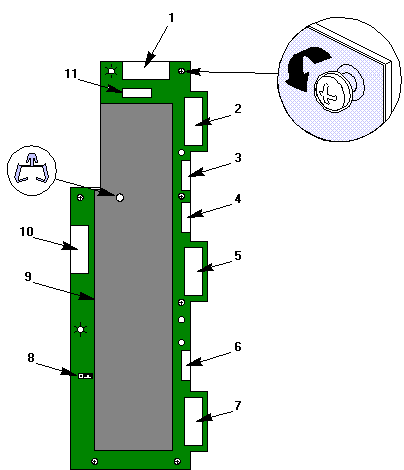
|
1 |
J1 output to system board |
7 |
J11 input from bottom power supply |
2 |
J3 input from top power supply |
8 |
J10 (factory configured jumper) |
3 |
J4 input from top power supply |
9 |
Non-removable cover |
4 |
J6 input from middle power supply if present |
10 |
J5 output to server peripherals |
5 |
J7 input from middle power supply if present |
11 |
J2 output to auxiliary power connector on system board |
6 |
J9 input from bottom power supply |
|
|
Power
The power sub system of the system is supplied in 2 configurations. 1)
Non load sharing and 2) Load sharing ( in redundant and non redundant configurations)
1) Non Load sharing
In this configuration a single PSU is connected to an internal wiring harness through
the Molex connection. This then supplies power to motherboard and disk sub systems. The
control connection from the PSU connects directly to the motherboard. This control
connector contains voltage remote sense lines, 5V Standby, Power On and Power Good
signals.
In this configuration the maximum systems configuration is limited to
300 Watts. This configuration is known as "Half Load" - which
limits the machine to supporting a maximum configuration of 5 Hard Disk Drives, 2 CPU's,
and 512MB.
2) Load Sharing
In this configuration the same PSU is connected to a load sharing PCB in the product.
This has provision for up to 3 PSU’s. From the Load sharing PCB connections are made
to the motherboard and drive sub systems. The maximum systems configuration is dependent
on the amount of PSU's present in the system. This configuration can either be redundant
or not. In order to be redundant then there must be 1 more PSU than the system needs to
power the configuration. These limits can be found by inputting the configuration of the
system into the power spreadsheet.
PSU Power
Each PSU ( Delta DPS333AB rev S3.P/N: 658841-004 ) is cable of the
following power limits from AC voltages 100 to 120Vac and 200 - 240Vac dependent on switch
selection of PSU ( 50 to 60 Hz).
| Power System Voltage |
+3.3V |
+5V |
+12V |
-5V |
-12V |
| Single PSU non load sharing |
11A |
32A |
12A |
0.25A |
0.5A |
| PSU’s in Load sharing configurations |
10A |
30A |
11A |
0.25A |
0.5A |
Each PSU produces a 0.1A standby power which supplies to
the management microcontrollers. PSU are controlled so that they can be soft started by
the system dynamically during operation of the system. Further the maximum power output is
actively limited to 240VA. Through the I2C bus The current levels in each output can be
measured. Each PSU will also indicate failure and presence to the load sharing board.
If a second power supply is fitted it will be fitted in the bottom PSU
position inside the chassis. If a third PSU is fitted it will replace the fan that was
fitted in the middle PSU position.
Cooling
In non load sharing configurations the PSU provides cooling with an
additional fan at the middle PSU addition site. These fans are connected back to the SCSI
backplanes for instrumentation.
Two fans will be fitted in the machine unless configured for redundancy,
then an additional 2 fans will be installed.
 
Add-Ins
| DIMM memory expansion |
|
| 32MB upgrade (1 x 32MB DIMM) |
XB57208 |
| 64MB upgrade (1 x 64MB DIMM) |
XB61639 |
| 128MB upgrade (1 x 128MB DIMM) |
XB61089 |
| Additional Processors |
|
| Single to dual Pentium Pro at 200MHz, 256KByte Cache |
XB61329 |
| Single to dual Pentium Pro at 200MHz, 512KBytes Cache |
XB61330 |
| Redundant Power Supply |
|
| N+1 Redundant power supply upgrade (includes 2 psu modules) |
XB100 |
| Additional power supply module for the above |
XB61332 |
| Network options |
|
| 3Com 10/100 PCI Ethernet card (3C905TX) |
XB59527 |
| 3Com PCI Ethernet Combo card (3C900) |
XB59526 |
| 3Com AUI to UTP Transceiver (3C583) |
XB50900 |
| Intel Pro 100B PCI Ethernet Card |
XB61343 |
| Intel Pro 10+ Combo ISA Ethernet Card |
XB61345 |
| Rack Mount Kit |
|
| Rack mount assembly for mounting server in 19" rack |
XB61584 |
| Controller cards for non-raid systems |
|
| Adaptec 2940uw + 2nd backplane for additional U/W SCSI channel |
XB200 |
| Cable kit for Adaptec 2940uw |
XB61348 |
| Controller cards for raid systems |
|
| AMI 428 2 channel raid |
XB61565 |
| Cable kit for AMI 428 |
XB61348 |
| 4MB AMI Raid Cache Upgrade |
XB61650 |
| DPT 3334uw 2 channel raid |
XB59763 |
| Cable kit for DPT 3334uw |
XB61348 |
| 4MB DPT Raid Cache Upgrade |
XB55494 |
| Server Management |
|
| Server Management Card |
XB61339 |
| Modem for the above (PCMCIA) |
XB61341 |
| UPS |
|
| APC 1000v/a smart ups |
XB60370 |
| Video Upgrade |
|
| 512KB to 1MB Video RAM |
XB61346 |
Hard Drives
| MB |
Make |
Model |
Type |
Part Number |
| 4GB |
IBM |
DCAS-34330 |
UltraSCSI |
XB61177 |
Tape Drives
Floppy Drives
| MB |
Make |
Model |
Type |
Part Number |
| 2 MB |
Mitsubishi |
355F-2450MP |
3.5" |
|
CD-ROM
| MB |
Make |
Model |
Type |
Part Number |
|
Sony |
CDU511-10/10 |
IDE PCAV |
XB61060 |
 
Jumper Settings
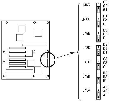
|
| Jumper |
Pins (default in bold) |
Resetting the server |
| J46G, Intrusion detect |
1-2, Enabled |
Activates alarm switches. They detect removal of the
chassis covers. |
| |
2-3, Disabled |
Bypasses the chassis intrusion switch. |
| J46F, Boot Option |
1-2, Normal |
Inverts address A16 so that the Normal BIOS does not
reside at the top of Flash memory where the write-protected Recovery BIOS region is
located. |
| |
2-3, Recovery |
Prevents inverting address A16. Allows the system to boot
from the Recovery BIOS when the normal BIOS gets corrupted, if you are unable to reload a
fresh copy from the floppy diskette. |
| J46E, Flash Control |
1-2, Erase/Program |
Applies +12 V power to the VPP pin on the Flash memory
device, and enables erasing or programming of Flash memory. |
| |
2-3, Protect |
Protects the contents of Flash memory. |
| J43D, Boot Block |
1-2, Erase/Program |
Permits boot block erasing and programming. |
| |
2-3, Protect |
Prevents writing to the BIOS boot block. |
| J43C, Fault Resilient Boot |
1-2, Enabled |
Allows the system to boot from processor 1 if processor 0
fails. |
| |
2-3, Disabled |
Lets the system boot only from processor 0. |
| J43B, Password Clear |
1-2, Protect |
Maintains the current system password. |
| |
2-3, Erase |
Clears the password. |
| J43A, CMOS Clear |
1-2, Protect |
Preserves the contents of NVRAM. |
| |
2-3, Erase |
Replaces the contents of NVRAM with the manufacturing
default settings. |
 
CMOS
The jumper on J43A pins 1 and 2 preserves the CMOS settings during
system reset. Moving the jumper to pins 2 and 3 clears CMOS and sets it and the real-time
clock (RTC) to the manufacturing default settings during system reset.
To reset the system’s CMOS and the RTC to factory default values:
Remove the left side cover.
Move the jumper on J43A from pins 1 and 2 to pins 2 and 3; replace the left side cover,
and connect the power cable(s) to the system.
Turn the system on, and wait for POST to complete. This automatically reprograms CMOS and
RTC to their default settings.
Turn the system off, disconnect the power cable(s) from the system, and remove the left
side cover again.
Move the jumper on J43A from pins 2 and 3 to pins 1 and 2; replace the left side cover,
and connect the power cable(s) to the system.
Run the SCU to configure your system.
 
System Resources
I/O Map
Address |
Resource
|
0000h–000Fh |
DMA Controller 1
|
0020h–0021h |
Interrupt Controller 1
|
002Eh–002Fh |
Super I/O Index and Data Ports
|
0040h–0043h |
Programmable Timer
|
0060h, 0064h |
Keyboard Controller
|
0061h |
NMI Status & Control Register
|
0070h |
NMI Mask (bit 7) & RTC Address (bits 6:0)
|
0071h |
Real Time Clock (RTC)
|
0080h–0081h |
BIOS Timer
|
0080h–008Fh |
DMA Low Page Register
|
0092h |
System Control Port A (PC-AT control Port)
|
00A0h–00BFh |
Interrupt Controller 2
|
00C0h–00DFh |
DMA Controller 2
|
00F0h |
Clear NPX error
|
00F8h–00FFh |
x87 Numeric Coprocessor
|
0170h–0177h |
Secondary Fixed Disk Controller (IDE)
|
01F0h–01F7h |
Primary Fixed Disk Controller (IDE)
|
0200h–0207h |
Game I/O Port
|
0220h–022Fh |
Serial Port A
|
0238h–023Fh |
Serial Port B
|
0278h–027Fh |
Parallel Port 3
|
02E8h–02Efh |
Serial Port B
|
02F8h–02FFh |
Serial Port B
|
0338h–033Fh |
Serial Port B
|
0370h–0375h |
Secondary Floppy
|
0378h–037Fh |
Parallel Port 2
|
03B4h–03BAh |
Monochrome Display Port
|
03BCh–03BFh |
Parallel Port 1 (Primary)
|
03C0h–03CFh |
Video Display Controller
|
03D4h–03DAh |
Colour Graphics Controller
|
03E8h–03EFh |
Serial Port A
|
03F0h–03F5h |
Floppy Disk Controller
|
03F6h–03F7h |
Primary IDE - Secondary Floppy
|
03F8h–03FFh |
Serial Port A (Primary)
|
0400h–043Fh |
DMA Controller 1, Extended Mode Registers
|
0461h Extended |
NMI / Reset Control
|
0462h |
Software NMI
|
0480h–048Fh |
DMA High Page Register
|
04C0h–04CFh |
DMA Controller 2, High Base Register
|
04D0h–04D1h |
Interrupt Controllers 1 and 2 Control Register
|
04D4h–04D7h |
DMA Controller 2, Extended Mode Register
|
04D8h–04DFh |
Reserved
|
04E0h–04FFh |
DMA Channel Stop Registers
|
0678h–067Ah |
Parallel Port (ECP)
|
0778h–077Ah |
Parallel Port (ECP)
|
07BCh–07BEh |
Parallel Port (ECP)
|
0800h–08FFh |
NVRAM
|
0CA4 |
PCI to IRQ rerouter control (PCI_INTB_L, PCI_INTA_L)
|
0CA5 |
PCI to IRQ rerouter control (PCI_INTD_L, PCI_INTC_L)
|
0CA6h–0CA7h |
Reserved
|
0CA9h |
DISMIC Data Register
|
0CAAh |
DISMIC Control/Status Register
|
0CABh |
DISMIC Flags Register
|
0C84h |
Board Revision Register
|
0C85h–0C86h |
BIOS Function Control
|
0CF8h |
PCI CONFIG_ADDRESS Register
|
0CF9h |
PMC Turbo and Reset control
|
0CFCh |
PCI CONFIG_DATA Register
|
46E8h |
Video Display Controller
|
xx00–xx1F* |
SCSI registers
|
*SCSI I/O base address is set using the
configuration registers.
Interrupts
INTR |
Processor interrupt. |
NMI |
NMI from DISMIC to processor. |
IRQ0/MIRQ0 |
System board interrupt request 0 connected to input 2 of
the I/O Apic. (For proper operation, the BIOS must set the IRQ0 enable bit in PIIX3
register 70h during initialisation.) |
IRQ1 |
RTC. |
IRQ3 |
Serial port A or B interrupt from 87307VUL device, user
configurable. |
IRQ4 |
Serial port A or B interrupt from 87307VUL device, user
configurable. |
IRQ5 |
Parallel port. |
IRQ6 |
Floppy diskette. |
IRQ7 |
Parallel port. |
IRQ8_L |
|
IRQ9 |
|
IRQ10 |
|
IRQ11 |
|
IRQ12 |
Keyboard/mouse interrupt from 87307VUL. |
IRQ14 |
Compatibility IDE interrupt from primary IDE devices 0 and
1. |
IRQ15 |
|
IDE_IRQ |
Tied to IRQ14; hard wired from PIIX3. |
The following signals will be
rerouted to the above interrupts:
PCI_INTA_L |
PCI Interrupt signal A from PIIX3. Wired to PCI-0 slot 1
INTA_L, PCI-0 slot 2 INTD_L, PCI-0 slot 3 INTC_L, PCI-0 slot 4 INTB_L, PCI-1 slot 1
INTA_L, and PCI-1 slot 2 INTD_L. |
PCI_INTB_L |
PCI Interrupt signal B from PIIX3. Wired to PCI-0 slot 1
INTB_L, PCI-0 slot 2 INTA_L, PCI-0 slot 3 INTD_L, PCI-0 slot 4 INTC_L, PCI-1 slot 1
INTB_L, and PCI-1 slot 2 INTA_L. This interrupt is also used by the SCSI controller. |
PCI_INTC_L |
PCI Interrupt signal C from PIIX3. Wired to PCI-0 slot 1
INTC_L, PCI-0 slot 2 INTB_L, PCI-0 slot 3 INTA_L, PCI-0 slot 4 INTD_L, PCI-1 slot 1
INTC_L, and PCI-1 slot 2 INTB_L. This interrupt is also used by the Network controller. |
PCI_INTD_L |
PCI Interrupt signal D from PIIX3. Wired to PCI-0 slot 1
INTD_L, PCI-0 slot 2 INTC_L, PCI-0 slot 3 INTB_L, PCI-0 slot 4 INTA_L, PCI-1 slot 1
INTD_L, PCI-1 slot 2 INTC_L. |
SMI_L |
System Management Interrupt. General-purpose error
indicator from a control PAL that provides an SMI_L from non-traditional error sources
(PERR_L, SERR_L, and others). |
| PCI Slot |
Will have the same IRQ as |
| 1 - 1 |
2 - 1 |
| 1 - 2 |
2 - 2 |
| 1 - 3 |
On-board Ethernet |
| 1 - 4 |
AIC 7880 |
 
POST Beep Codes
Beeps |
Error Message and Conditions |
1 |
Refresh failure; memory refresh circuitry on the baseboard
is faulty |
2 |
ECC double-bit error can not be reset |
3 |
First 64 KB memory failure |
4 |
Timer not operational; timer on baseboard not operational
or memory failure in first 64 KB memory |
5 |
Processor failure; processor on the processor/memory
module generated an error |
6 |
Keyboard controller gate A20 is off; BIOS cannot switch to
protected mode. Keyboard controller may be bad. |
7 |
Processor exception interrupt error |
8 |
Display memory read/write error; system video adapter is
missing or its memory is faulty (not a fatal error) |
9 |
ROM checksum error; ROM checksum value does not match
encoded value in BIOS |
10 |
Shutdown register read/write error; shutdown register for
CMOS RAM failed |
 

|


